
DC production testing of telecommunications laser diode modules

Contents
• Introduction
• Test descriptions
• Test system configuration
• System expansion
• Methods and techniques
• Typical sources of error
• Equipment list
• Test system safety
• For further reading
Introduction
The ever-increasing demand for communications bandwidth is accelerating the demand for telecom laser diode (LD) modules. As volume production and the complexity of the LD modules increases, a greater emphasis is placed on cost-effective and accurate production test strategies. The typical LD module consists of a laser diode and a back facet monitor photodiode. Temperature-controlled LD modules also include a thermo-electric controller (TEC) and a thermistor to simplify precise regulation of the LD's operating temperature, as shown in Figure 1.
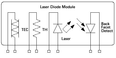
Note: High-speed LD modules can also include an integrated modulator chip, which is not illustrated in Figure 1.
The valued-added nature of the LD assembly dictates testing each component prior to the next assembly step. For instance, the cost of repairing or scrapping a complete laser module due to a failed back facet monitor photodiode is much greater than the cost of providing 100% testing of the photodiode component prior to the assembly step. To reduce the cost of the test, high-speed flexible test solutions are needed. This application note details a cost-effective DC test system that provides the high-volume throughput required in today's telecom LD transceiver module production environments.
Back to top
Test descriptions
Specifications provided in the typical distributed feedback (DFB) laser diode module of interest during DC testing include:
- Laser diode forward voltage
- Kink test and slope efficiency (dL/dI)
- Threshold current
- Monitor (back facet) current
- Optical output power
- Monitor (back facet) voltage drop
- Monitor (back facet) dark current
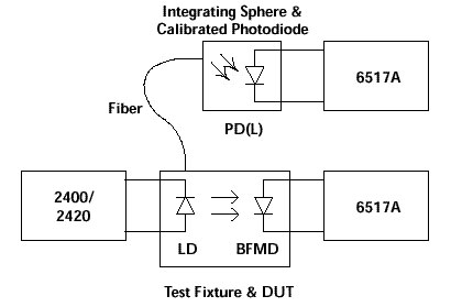
The most common subset of the DC characteristics (the first five tests listed) can be measured in a test sequence known as the L-I-V Test Sweep. This fast (less than 10 seconds for a 100-point sweep at 1 NPLC, excluding analysis time) and inexpensive DC test identifies failed assemblies early in the test process, so that expensive non-DC domain test systems can be more cost-effective on the remaining higher-yield components. Figure 2 illustrates an example application that configures three instruments to perform the L-I-V test sweep.
L-I-V test sweep
Forward voltage test
The forward voltage (VF ) test verifies the forward DC characteristics of the LD. Current (IF ) is swept and the voltage drop across the LD is measured. Some high-powered LDs may require current (IF ) sweeps of up to 2 to 3A, usually in increments of 1mA. Most need sweeps of up to 1A. The time required for a test sweep should be in the range of a few milliseconds. The typical measurement range is 0–10V and microvolt-level resolution is required.
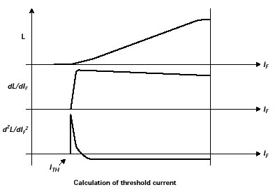
Lasing threshold current test
The threshold current is the current at which the LD starts lasing. The current threshold can be found by detecting the first maxima of the second derivative of the light output. Figure 3 shows the graphic calculation of the threshold current of an LD. The top line is the light output of the LD as the current is swept from zero to several tenths of an ampere. The middle line is the first derivative of the light output and shows a steep slope as the light output begins to intensify. The bottom line is the second derivative of the light output. Note the sharp peak of the second derivative line at the knee of the light intensity output. This peak denotes the location of the threshold current.
Light intensity measurement
Light intensity (L) measurements verify the light output of the LD. Light output power increases as drive current is increased. Results of this test are usually displayed in mW to W. The measurement may be AC- or DC-based. For AC-based measurements, an optical power meter is used. For DC-based measurements, a reverse-biased photodiode is exposed to the output of the laser diode, and the resulting photodiode DC current is measured with a picoammeter or electrometer (highly-refined DC multimeter). The system software then uses this current value and the PD calibration data to calculate the output power of the module. A typical photodiode current range is 0–3mA. Required resolution is 100nA. The DC approach is reportedly faster than the AC approach.
Back facet monitor diode (BFMD) test
This test verifies the response of the back facet detector pho-todiode (also reverse biased) to increased light output of the LD as the drive current is increased. The typical current measurement range is 0–100mA and the required resolution is 100nA. This measurement is typically performed with a picoammeter or electrometer.
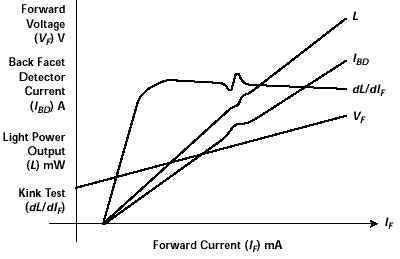
Kink test/slope efficiency
This test verifies the proportionality of the relationship between the drive current (IF ) and the light output (L) as depicted in Figure 4. The relationship between the drive current (IF ) and the light output power (L) should be linear throughout the nominal operating range. If the relationship is truly linear over the tested range, the first derivative of the curve will be a nearly horizontal line. This is graphed as dL/dIF . The first derivative will tend to amplify any bumps or kinks in the L–IF curve. If this curve has any significant "kinks" (if the curve is not smooth), the laser is considered defective. If operated at the IF value corresponding to the "kink," the light output will not be proportional. The maximum value of the second derivative of the L vs. IF curve can be used to calculate the threshold current.
Back to top
Test system configuration
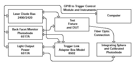
Figure 5 shows the basic core of a test system consisting of one Model 2400 SourceMeter instrument, two Model 6517A electrometers, and a PC equipped with a GPIB interface card. (If the LD modules require more than 1A but less than 3A of drive current, substitute the Model 2420 SourceMeter instrument for the Model 2400.) The Model 2400 is programmed to provide a current sweep to drive the LD and to synchronize the measurements made by the Model 6517A electrometers via the Trigger Link cables and Trigger Link Adapter box. The PC programs the meters via the GPIB bus, coordinates the execution of the test, and collects and analyzes the measurement results. Each instrument is equipped with a data buffer (sometimes called a trace memory) that allows readings to be stored internally until the test is complete. This data buffer, in conjunction with Trigger Link, allows the L-I-V test sweep to run at hardware speeds independent of the PC and GPIB interface. Once the test is complete, the readings in the data buffer are collected via the GPIB and analyzed in the PC.
Test sequence
With the LD in the test fixture socket, the operator initiates the L-I-V test sequence via the control computer.
1. The computer configures the bias of the LD laser, LD BFMD, and external photodetector (PD).
2. The instrument outputs are enabled and the Model 6517A electrometers are armed.
3. The Model 2400 is then triggered and the sweep begins.
4. As the Model 2400 (laser diode bias) sweeps from zero to 1A in 10mA steps, it signals when the next bias current is stable by issuing a trigger to the Model 6517A electrometers. The Model 2400 then records the current and voltage measurements in the data buffer for later recall by the computer.
5. The Model 6517A electrometers measure the current flow in the photodiodes and issue triggers to the Model 2400. The measurements are recorded in the data buffer.
6. The trigger signals from the electrometers signal the Model 2400 to increase the LD laser bias to the next step.
7. The exchange of triggers synchronized by the Model 2400 repeats until all measurements in the sweep are complete.
8. When the Model 2400 signals the completion of the L-I-V test sweep, the computer disables the output of the instruments, reads the measurements from the data buffer, and compiles the test results.
24xx setup
A linear staircase sweep is easily programmed using the following standard commands for programmable instruments (SCPI) command sequences:
‘Reset 2400
send (kth2400, "*rst", status)
send (kth2400, ":syst:beep:stat off", status)
send (kth2400, ":syst:azer:stat off", status)
‘Use Rear Terminals
send (kth2400, ":rout:term rear", status)
‘Configure Sense Circuit
send (kth2400, ":sens:volt:nplc 0.01", status)
send (kth2400, ":sens:func:conc off", status)
send (kth2400, ":sens:func volt:dc'", status)
send (kth2400, ":sens:volt:prot 0.001", status)
send (kth2400, ":form:elem volt", status)
‘Configure Source Circuit
send (kth2400, ":sour:func curr", status) ‘source amps
send (kth2400, ":sour:curr:start 0.010", status) ‘start at 10 milliamps
send (kth2400, ":sour:curr:stop 1", status) ‘end at 1A
send (kth2400, ":sour:curr:step 1e-2", status) ‘increment in 10mA steps for a total of 100 steps
send (kth2400, ":sour:curr:mode sweep", status) ‘set sweep mode
send (kth2400, ":sour:swe:rang auto", status)
send (kth2400, ":sour:swe:spac lin", status) ‘set step spacing to linear
send (kth2400, ":sour:del 0.002", status) ‘set delay before trigger is sent to 6517a
'Configure Arm Layer Setup
send (kth2400, ":arm:sour tlink", status) ‘Trigger Link will be trigger source
send (kth2400, ":arm:ilin 3", status) ‘input trigger will be line 3
send (kth2400, ":arm:dir source", status) ‘bypass trigger once
send (kth2400, ":arm:count 1", status) ‘trigger count = number of measurements
'Configure Trigger Layer Setup
send (kth2400, ":trig:clear", status) ‘clear triggers
send (kth2400, ":trig:sour tlink", status) ‘Trigger Link will be trigger ‘source
send (kth2400, ":trig:ilin 1", status) ‘input trigger will be line 1
send (kth2400, ":trig:olin 2", status) ‘output trigger will be line 2
send (kth2400, ":trig:outp delay", status) ‘send trigger after source 'and delay steps
send (kth2400, ":trig:dir source", status) ‘bypass trigger once
send (kth2400, ":trig:count 100", status) ‘trigger count = number of measurements
‘Configure Trace
send (kth2400, ":trace:point 100", status) ‘store 100 readings
send (kth2400, ":trace:feed sens", status) ‘store readings
send (kth2400, ":trace:feed next", status) ‘enable trace
The Model 2400 is programmed to sweep from 10mA to 1000mA in 100 steps of 10mA each. After each new current value is applied to the LD, a trigger is issued on Trigger Link (tlink) line 2 to start the measurement sequence on the Model 6517A electrometers that measure light output by measuring photodiode current. The Model 2400 waits in the Arm Layer for a trigger on Trigger Link line 3 from the electrometer designated 6517A-2, then waits for a Trigger Layer trigger from Trigger Link line 1 from the electrometer designated 6517A-1. (Trigger Link inputs are edge sensitive and latch incoming triggers to allow asynchronous triggering. This feature allows the Trigger Layer trigger to be issued before the Arm Layer trigger without disrupting the flow of the test.)
6517A-1 setup
Both of the Model 6517A electrometers are programmed to wait for a trigger on Trigger Link line 2 from the Model 2400 to begin a measurement cycle. The first Model 6517A (6517A-1) is set up to issue a trigger on Trigger Link line 1 after a reading has been stored in the data buffer. The second Model 6517A (6517A-2) is programmed in exactly the same way as the first, except the output trigger is directed to Trigger Link line 3.
‘Reset Instrument
send (kth6517A1, "*rst", status)
send (kth6517A1, "*cls", status)
‘Configure for faster measurements
send (kth6517A1, ":syst:zcheck on", status)
send (kth6517A1, ":syst:hlc on", status)
send (kth6517A1, ":form:elem read", status)
send (kth6517A1, ":calc1:state off", status)
send (kth6517A1, ":calc2:state off", status)
‘Configure Sense Circuit
send (kth6517A1, ":sens:func ‘dc:curr'", status)
send (kth6517A1, ":sens:curr:dc:nplc 1", status)
send (kth6517A1, ":sens:curr:dc:aver:state off", status)
send (kth6517A1, ":sens:curr:dc:rang:auto on", status)
send (kth6517A1, ":sens:curr:dc:range:auto:llimit 1e-07", status)
‘Configure Source Circuit
send (kth6517A1, ":sour:volt:range 100", status)
send (kth6517A1, ":sour:volt 5", status)
send (kth6517A1, ":sour:volt:mconnect on", status)
‘Configure Arm Layer 1 to be bypassed
send (kth6517A1, ":arm:lay1:sour imm", status)
send (kth6517A1, ":arm:lay1:count 1", status)
send (kth6517A1, ":arm:lay1:tcon:dir source", status) ‘set bypass
‘Configure Arm Layer 2 to be bypassed
send (kth6517A1, ":arm:lay2:sour imm", status)
send (kth6517A1, ":arm:lay21:count 1", status)
send (kth6517A1, ":arm:lay21:tcon:dir source", status) ‘set bypass
‘Configure Trigger Layer to slave to Trigger Link
send (kth6517A1, ":trig:sour tlink", status) ‘Trigger Link will be trigger source
send (kth6517A1, ":trig:tcon:prot asyn", status) ‘trigger will be ‘asynchronous
send (kth6517A1, ":trig:tcon:asyn:olin 1", status) ‘output triggers on line 1
send (kth6517A1, ":trig:tcon:asyn:ilin 2", status) ‘input triggers on line 2
send (kth6517A1, ":trig:tcon:dir acceptor", status) ‘not bypassed, trigger required to advance
send (kth6517A1, ":trig:count 100", status) ‘number of ‘measurements
‘Record measurements to trace memory
send (kth6517A1, ":trace:clear", status)
send (kth6517A1, ":trace:points:auto 1", status)
send (kth6517A1, ":trace:feed:control next", status)
6517A-2 setup
‘Reset Instrument
send (kth6517A2, "*rst", status)
send (kth6517A2, "*cls", status)
‘Configure for faster measurements
send (kth6517A2, ":syst:zcheck on", status)
send (kth6517A2, ":syst:hlc on", status)
send (kth6517A2, ":form:elem read", status)
send (kth6517A2, ":calc1:state off", status)
send (kth6517A2, ":calc2:state off", status)
‘Configure Sense Circuit
send (kth6517A2, ":sens:func ‘dc:curr'", status)
send (kth6517A2, ":sens:curr:dc:nplc 1", status)
send (kth6517A2, ":sens:curr:dc:aver:state off", status)
send (kth6517A2, ":sens:curr:dc:rang:auto on", status)
send (kth6517A2, ":sens:curr:dc:range:auto:llimit 1e-07", status)
‘Configure Source Circuit
send (kth6517A2, ":sour:volt:range 100", status)
send (kth6517A2, ":sour:volt 5", status)
send (kth6517A2, ":sour:volt:mconnect on", status)
‘Configure Arm Layer 1 to be bypassed
send (kth6517A2, ":arm:lay1:sour imm", status)
send (kth6517A2, ":arm:lay1:count 1", status)
send (kth6517A2, ":arm:lay1:tcon:dir source", status) ‘set bypass
‘Configure Arm Layer 2 to be bypassed
send (kth6517A2, ":arm:lay2:sour imm", status)
send (kth6517A2, ":arm:lay21:count 1", status)
send (kth6517A2, ":arm:lay21:tcon:dir source", status) ‘set bypass
‘Configure Trigger Layer to slave to Trigger Link
send (kth6517A2, ":trig:sour tlink", status) ‘Trigger Link will be trigger source
send (kth6517A2, ":trig:tcon:prot asyn", status) ‘trigger will be ‘asynchronous
send (kth6517A2, ":trig:tcon:asyn:olin 3", status) ‘output triggers on line 1
send (kth6517A2, ":trig:tcon:asyn:ilin 2", status) ‘input triggers on line2
send (kth6517A2, ":trig:tcon:dir acceptor", status) ‘not bypassed, trigger 'required to advance
send (kth6517A2, ":trig:count 100", status) ‘number of ‘measurements
‘Record measurements to trace memory
send (kth6517A2, ":trace:clear", status)
send (kth6517A2, ":trace:points:auto 1", status)
send (kth6517A2, ":trace:feed:control next", status)
Start sweep
To start the sweep, the outputs of all the instruments are first turned on. Then, the Model 6517A electrometers are armed and wait for a trigger from the Model 2400. Finally, the Model 2400 receives an initialization command (:init) from the controlling PC over the GPIB bus.
‘Enable outputs
send (kth6517A1, ":outp on", status) ‘bias photodiode
send (kth6517A2, ":outp on", status) ‘bias photodiode
send (kth2400, ":outp on", status) ‘bias LD
send (kth6517A1, ":init", status) ‘arm
send (kth6517A2, ":init", status) ‘arm
send (kth2400, ":init", status) ‘trigger sweep
send (kth6517A1, ":outp off", status) ‘turn outputs off
send (kth6517A2, ":outp off", status)
send (kth2400, ":outp off", status)
Read trace buffers
‘query trace buffers
send (kth6517A1, ":trace:data?", status)
send (kth6517A2, ":trace:data?", status)
send (kth2400, ":trace:data?", status) ‘enter data
send (strData, 2000, intLength, kth6517A1, status)
send (strData, 2000, intLength, kth6517A2, status)
send (strData, 2000, intLength, kth2400, status)
Pass/fail analysis
Three data streams (the forward voltage trace, the LD back facet detector current trace, and the external photodiode current trace) are mathematically manipulated to quantify the threshold current, quantum efficiency, and maximum differential ohms excursion. These numbers are compared to expected values to determine the quality of the LD.
Depending on the noise content of the data streams, it may be necessary to perform filtering operations before performing calculations such as dL/dIF. The low-noise characteristics of the Series 2400 SourceMeter line and Model 6517A electrometers reduce the need for noise compensation techniques. Keithley has developed an example Microsoft VisualBasic program that illustrates how to perform an L-I-V Test Sweep with a Model 2420 SourceMeter instrument and two Model 6517A electrometers. To download a copy of the program (LIVTestSweep.zip) visit Keithley's web site (http://www.keithley.com).
Back to top
Telecom LD module pinouts
Telecom LD modules from a given manufacturer often have more than one pinout configuration. By routing all the instrumentation signals through a Keithley Model 7002 Switch Mainframe equipped with an appropriate switch card, various LD module pinouts can be easily accommodated via computer control. The switch also allows these instruments to make complex isolation and quiescent power measurements.
Modulation inputs
LD modules are often equipped with modulation or attenuation control inputs. The addition of a second Model 2400 to bias the attenuation input may be required to perform the basic L-I-V test sweep. The bias value is held constant during the L-I-V test sweep, so the SourceMeter instrument should not be part of the Trigger Link interconnect.
Forward voltage test
The forward voltage is the result of the majority carrier current flow; therefore, it is a function of the semiconductor material and the temperature of the junction. The forward voltage test can be performed on the LD as well as on the back facet photodiode to determine the forward operating voltage of the semiconductor junction. Typically, a Series 2400 SourceMeter instrument is configured to source a sufficiently small current (to prevent damage) and to measure the resulting voltage across the junction. Given that most detectors use semiconductor materials with temperature coefficients of about 2mV/°C, the temperature of the junction must be known or controlled.
Reverse-breakdown voltage test
As the reverse-bias voltage is increased, the velocity of the minority carriers crossing the junction is increased. At a given reverse voltage, the energy of the charge carriers is sufficient to result in ionization by collision. This voltage is known as the reverse-breakdown voltage. If the current at this voltage is carefully limited, the junction will not be destroyed. The reverse-breakdown voltage test can be performed on the LD and on the back facet photodiode. A non-destructive reverse-breakdown test can be performed by sourcing –10µA and measuring the resulting junction voltage. The Model 2400 SourceMeter instrument is ideal for this measurement.
Leakage current test
The reverse-biased semiconductor junction (at less potential than the breakdown voltage) has a leakage current that is made up of minority carriers crossing the depletion region. The magnitude of the leakage current is dependent on electronic charge, doping density, junction area, and temperature. Leakage currents of the laser diode and the back facet photodiodes can be tested with a Model 2400. Typically, 80% of the reverse-breakdown voltage is applied to the junction, and the resulting leakage current is measured. For the photodiode, this test also serves as the dark-current measurement. With the LD bias held to zero, the dark current is measured by applying a bias to the junction and measuring the current flow. During this measurement, it is critical to prevent any stray photons from impinging on the LD and back facet photodiode.
Thermistor test
The thermistor of a typical LD module has a nominal resistance of 10kohmsat 25°C. In normal operation, the thermal stability of the module is more critical than the absolute temperature value. A number of techniques can be used to test the thermistor:
1. Hold the temperature of the LD module to a known value and measure the resistance of the thermistor.
2. Thermally couple a characterized thermistor to the LD module, allow the assemblies to reach a thermal equilibrium, and compare the characterized thermistor resistance with the LD thermistor resistance.
3. Set a wide enough range of resistance values to accommodate the temperature of the LD module in the manufacturing process. To avoid self-heating of the thermistor, if is important to keep power dissipation to a minimum. Typically, a constant current of 10µA to 100µA is sourced, and the resulting voltage measurement is used to derive resistance.
Thermoelectric cooler (TEC) test and control
Many LD modules are equipped with a thermoelectric cooler (Peltier device). Typically, a TEC controller is used to control the temperature of the module during the L-I-V test sweep. It is also possible to verify the functionality of the TEC device by modulating the temperature set point and verifying the thermistor resistance after the new temperature is reached. Perhaps the most common failure mechanism in Peltier devices is excessive mechanical shear loads. During the handling and mounting of the Peltier device, mechanical shear loads can cause de-lamination or breakage of some or all of the elements in the device. A simple AC or reversing DC resistance test can determine the health of the Peltier device before and after mounting in the LD module. A direct current resistance measurement would include errors due to self-heating of the elements and the resulting thermal offsets. The Model 2400 can provide the necessary bipolar current source and voltage measurement capability to simplify this measurement.
Isolation test
Using a switch matrix makes it easier to perform isolation tests between the various components of the LD module. For instance, the electrical isolation of the thermistor from the LD can be tested by applying a potential between the thermistor and LD while holding both terminals of the thermistor and both terminals of the LD at the same potential to prevent current flow through the individual components.
Back to top
Model 2361 trigger controller
As additional test capabilities are added to the basic test system core, the control and coordination of triggers can grow beyond the capability of the trigger control circuits supported in the individual instruments. The Model 2361 Trigger Controller provides system-wide trigger control with a dedicated programmable trigger control micro-sequencer, six input trigger lines, and six output trigger lines. The Trigger Controller's microsequencer provides high-level control, including looping, loop repeat, trigger repeat, and memory control. Once programmed, the Trigger Controller executes independently of the host computer. This allows faster and more predictable operation than can be achieved with GPIB bus commands. Refer to Keithley's Website for application notes on Trigger Link programming.
Contact check
The contact check option, available on the Series 2400 SourceMeter line, helps eliminate measurement errors and false failures by verifying the resistance between Output HI/Sense HI, Output LO/Sense LO, and Guard/Guard Sense connections. Contact check uses a pulse scheme that minimizes the potential at the DUT during the resistance measurement, verifies all three resistance values simultaneously, and requires less than 1ms per DUT.
Cabling
Cabling must be optimized for accuracy and test speed. High-quality, low-noise cable is required for all measurements. The cable characteristics for the LD drive signal are very different than those of the photodiode signals. The photodiode signal is generated by sourcing several volts and measuring the current flow in the microampere range. It is critical that a low-noise shielded cable be used to optimize the signal-to-noise ratio at such low currents. Using the shortest length of cable will also improve the signal-to-noise ratio by reducing leakage and induced currents, as well as minimizing capacitance. The slew rate (dV/dt) of the LD drive signal is a function of the semiconductor junction. The junction voltage will change only a few millivolts for a current change of tens of milliamps.
As a result of the low slew rate requirements, the capacitance of the LD drive signal cable is not as critical to the application as the voltage drop across the cable, as it carries up to 3A. A large gauge cable will help reduce the voltage drop over the length of the cable, while having minimal impact on the speed of the test. In all cases, the cabling must be shielded and kept as short as possible to reduce noise and capacitance. The lower the noise, the shorter the integration time required for each measurement, and the higher the test sweep speed.
Back to top
Leakage currents
During low-current measurements, or when using low-current photodiodes, techniques to minimize leakage may be required. In addition to the nominal leakage characteristics of the cabling and DUT fixturing, conductive contamination of the fixture will build over time and increase leakage currents. One technique for minimizing the leakage current is to use a guarded fixture. In a guarded fixture, the region near the DUT is held at the same potential as the Output HI signal, which reduces the potential difference between the DUT and the leak-age paths.
A more detailed explanation of the Guard and Guard Sense signals can be found in the white paper titled Obtaining More Accurate Resistance Measurements Using the 6-Wire Ohms Measurement Technique, available on the Test and Measurement.com Website.
Electrostatic interference
High-resistance measurements, like those made using photodiodes, may be affected by electrostatic interference from charged objects. An electrostatic shield (Faraday cup) may be required to eliminate electrostatic effects. For more information, refer to "Section 2.3: Low Current Measurements" in Keithley's hand-book, "Low Level Measurements."
Light interference
Stray light entering the optical fiber or the integrating sphere will skew the test results. Care must be taken to ensure that all components are properly shielded at all wavelengths that could affect the conductance of the semiconductor junctions. This is especially critical for dark-current measurements of the photodiode.
Back to top
Basic equipment:
- Model 2400/2420 SourceMeter instrument (Laser Diode Bias)
- Model 6517A Electrometer (Light Output Power)
- Model 6517A Electrometer (Back Facet Detector)
- Model 7008-3 IEEE-488 (GPIB) Cable (three required)
- Model KPC-488.2AT (or other IEEE-488 interface card)
- Model 8502 Trigger Link Adapter Box
- Model 8503 DIN-to-BNC Trigger Cable (two required)
- Model 8501-1 Trigger Link Cable
Expansion equipment:
- Model 2400 SourceMeter instrument (Modulator Bias)
- Model 2000 DMM (Resistance/Voltage Measurements)
- Model 7002 Switching System Mainframe
- Model 7053 High Current Switch Card
- Model 7012 4X10 Matrix Switch Card
- Model 2361 Trigger Controller
- TEC Controller
A suitable PC and software are also required to perform an L-I-V test sweep.
Note: For certain photodetector current measurement ranges, a Model 2400 SourceMeter instrument can be substituted for the Model 6517A electrometer.
Back to top
Test system safety
Under normal operating conditions, optical fiber communications systems employing a laser diode module are considered safe. However, during the testing of laser diode modules, care must be taken in ensure operator safety. Please consult your facility's laser safety officer or appropriate regulatory, health, and safety organizations.
Many electrical test systems or instruments are capable of measuring or sourcing hazardous voltage and power levels. It is also possible, under single fault conditions (for example, a programming error or an instrument failure), to output hazardous levels even when the system indicates no hazard is present. These high voltage and power levels make it essential to protect operators from any of these hazards at all times.
Protection methods include:
- Design test fixtures to prevent operator contact with any hazardous circuit.
- Make sure the device under test is fully enclosed to protect the operator from any flying debris. For example, capacitors and semiconductor devices can explode if too much voltage or power is applied.
- Double insulate all electrical connections that an operator could touch. Double insulation ensures the operator is still protected, even if one insulation layer fails.
- Use high-reliability, fail-safe interlock switches to disconnect power sources when a test fixture cover is opened.
- Where possible, use automated handlers so operators do not require access to the inside of the test fixture or have a need to open guards.
- Provide proper training to all users of the system so they understand all potential hazards and know how to protect themselves from injury.
It is the responsibility of the test system designers, integrators, and installers to make sure operator and maintenance personnel protection is in place and effective.
Back to top
For further reading
Keithley Instruments, Inc."Low Level Measurements: Precision DC Current, Voltage and Resistance Measurements." Fifth Edition. Cleveland, OH. 1998. (Available free upon request.)
Back to top