
Basics of Low Current Probing

This technical feature describes the fundamentals of making low current (femtoampere level) measurements using a probe station. Proper set up, shielding and guarding considerations are discussed. Equipment needs to provide the correct probing environment are described. The application note discusses a series of problem areas typically encountered when doing low current probing and recommends solutions to these problems.
Contents
•Representative low current measurements
•Source measure units
•Factors affecting the low level environment
•Guidelines for successful low level measurements
•Further Reading
•Acknowledgements
The need to observe device behavior at femtoampere (fA) levels is driven by the ongoing reduction in the geometric size of MOSFET devices to increase circuit density, facilitate higher speeds, and reduce power consumption. Decreasing the scale of the circuit can help provide the aforementioned improvements, but tradeoffs in performance will also occur. Tools must be available to observe the new operating characteristics for comparison with the predicted values. The measurement of current values in the range of 1 to 100 fA is difficult because many interfering sources exist that are capable of generating this minuscule flow of electrons. Consider that 1 fA (1x10-15 ampere) is equal to a flow rate of 6,242 individual electrons per second compared to the 6.242x10¹⁸ electrons per second that defines an ampere. Care and deliberation are required to setup a system capable of measuring currents down to these delicate levels.
Representative low current measurements
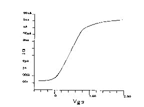
This article describes the grounding and shielding techniques needed for low current measurements using two typical probe contact configurations: surface-to-surface and surface-to-substrate. In the examples to follow, the surface-to-surface configuration will be represented by MOSFET subthreshold measurements and the surface-to-substrate measurements by time-dependent dielectric leakage observations (TDDL) (Figure 1). Subthreshold measurements (Figure 2) permit the analysis of drain current behavior below the gate turn on voltage. This off state drain current is typically much less than 100 femtoamperes and will influence DRAM memory refresh requirements.
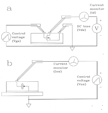
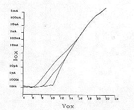
TDDL characterization (Figure 3) describes gate oxide leakage under the influence of high electric field stress. This behavior is of interest for the reliability of EPROM and flash memory devices because write/erase cycles will cause an increase in leakage current over time. Leakage current will be in the femtoampere range and can influence component leakage and other aspects of device performance resulting in eventual circuit failure.
Source Measure Units
Subthreshold and TDDL characteristics both require a voltage for the stimulus or source which produces a current as the response or measured value. A source measure unit (SMU) commonly facilitates this stimulus and response function. A SMU can be configured to:
- Source current and measure voltage
- Source voltage and measure current
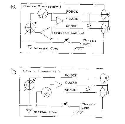
SMUs have two features that facilitate measurement accuracy. When IR drops in the cabling between the SMU and the device under test (DUT) are a concern, remote voltage sensing is available. If leakage paths and stray capacitive charging in the fixturing approach expected DUT current levels, a guard voltage output can minimize the influence of these paths. Figure 4 shows the configurations that will be used in the examples to follow.
Factors affecting the low level environment
A number of factors can adversely affect your low-level measurements. The very brief descriptions that follow are provided to help you form an intuitive basis for identifying and minimizing either the noise source or the noise coupling mechanism. Use these descriptions to visualize the relationships between noise and signal and to alter your experimental measurement setup to better isolate the noise from the signal. For more detailed information on the mechanisms described, refer to the reference texts listed at the end of this paper.
The noise coupling mechanisms are best described as "virtual components" in that they will not be obvious or localized as would a lumped equivalent component.
Common impedances
A common impedance is an impedance or current path unintentionally shared by a source of noise and the receiving instrumentation. The noise source causes current to flow through the common impedance. If this common impedance is in parallel with the instrument's input, a noise voltage will be coupled into the measured signal with the relationship:
Vnoise = i noise (Z coupling)
If the instrument is measuring current, then the current flowing through the common impedance will algebraically sum with the signal current at the connecting node.
Prevention measure: Analyze the grounding scheme and verify it conforms to single point grounding practice. Confirm that current paths between different circuit functions are isolated. Inspect the physical test setup and eliminate all casual, unintended contact between ground conductors that reside in different electrical parts of the circuit.
Incidental mutual inductance
Transfer of a noise voltage can occur through mutually coupled inductances in the noise circuit and the signal circuit. This inductive coupling will have the relationship:
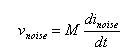
M is the mutual coupling between the noise circuit and signal circuit and will be influenced by proximity and shared length of noise and signal conductors. Vnoise is the noise voltage coupled into the signal circuit and is proportional dinoise/dt, which is the time derivative of the noise current.
Prevention measure: Eliminate common runs of conductors and cables, especially conductors not a part of the test signal circuitry. Maintain wide conductor spacing where possible. Isolate circuits with magnetic shielding where practical.
Magnetically coupled noise
Typical noise sources that lend themselves to magnetic coupling are motors, transformers and facility wiring. The coupling mechanism can be expressed as:
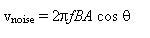
f is the frequency of the noise signal, B is a measure of the noise magnetic field strength, A is the area of a closed loop in the signal circuit and q (theta) is the angle of B to the plane of the loop area A.
Prevention measure: Remove unnecessary sources of electromagnetic energy in the area of the test circuit. Eliminate circuit loops. Magnetically shield wires or use twisted pairs.
Incidental capacitive coupling
A source of noise current can be coupled to the measurement circuit via stray capacitance according the relationship:
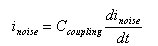
Ccoupling is the stray capacitance between the noise source and the measurement circuit. This noise current will be proportional to the voltage rise and fall times of the adjacent noise signal and proportional to the amount of stray capacitance between noise conductor and signal conductor. Stray capacitance is inversely proportional to the distance between conductors. If the circuit of interest has a high impedance, it will see a noise voltage. If the impedance is low, a current will be developed.
Prevention measure: Add distance between unshielded noise sources and the test circuit. Separation of two wires by a distance greater than 40 diameters will provide good electrostatic isolation.
Ensure the test circuit conductors are shielded to redirect capacitively coupled current away from the test circuit to ground. Active guard shields will also provide good protection.
Charge transfer
If a charged body is brought in proximity to the test circuit, that charge will attract or repel charge in the test circuit and cause momentary electron flow. This will perturb femtoampere measurements. A human body is the typical charge vehicle.
Prevention measure: Limit activity in the area of the test setup during measurements. Provide broad electrostatic isolation by using a metallic light tight enclosure (LTE). Run interconnecting cables between the LTE and SMU behind the test bench away from traffic and AC power cords.
Stray capacitance charging
The voltage supplied by the SMU for subthreshold and TDDL measurements will typically be a stepped sweep of increasing voltage over time. Stray capacitance in the cables and shield surfaces between the SMU and DUT must be charged which will introduce an added current that will swamp the DUT current. For low current measurements, this will be a major source of error.
Prevention measure: Use an active guarded shield on all cables to keep the differential charging voltage to a very small level. Use probes or probe holders that have guard shielding as close as practical to the probe point. Evaluate the settling time requirement after guarding is in place, and be sure to program an adequate measure delay time into the SMU.
Light
Semiconductor devices can be light sensitive. This is especially true for MOSFET devices that rely on minority carriers for conduction. At femtoampere levels, the currents induced by exposure to light will obliterate many measurements.
Prevention measure: Use a light tight enclosure (LTE) to provide a dark environment around the DUT. This serves to block all forms of electromagnetic radiation, not just the visible spectrum.
Intrinsic noise sources
At low femtoampere levels, most coaxial and triaxial cables will show current developed by triboelectric effects caused by flexing or vibration of the cable. Contacts between dissimilar metals as might be found in connectors, crimp joints or solder joints will develop temperature sensitive Seebeck voltages (thermal noise). Moisture combined with chemical residue left over from an assembly process can produce an electrochemical voltage.
Prevention measure: Minimize triboelectric errors by allowing cables to relax after installation. Anchor cables to prevent motion. Prevent Seebeck effect and electrochemical voltages by making connections with similar metals, and keeping connectors clean and dry.
Leakage current
All insulation used in cabling, connectors and probes will permit a degree of leakage that can influence femtoampere measurements. Some of this leakage is inherent to the insulating material, and additional leakage may sometimes be contributed by contamination during assembly or handling.
Prevention measure: Use an active guarded shield on all cables to keep the differential voltage to a very small level.
Guidelines for successful low level measurements
Pay attention to the details
Because of the very small physical values being observed, many factors can interfere with the desired measurements. It's important to review and practice the above prevention measures to eliminate problems before they occur.
Diagnose noise sources and minimize their effects
The biggest difficulty in solving noise problems at femtoampere levels is that analog time domain measurement techniques that will permit direct observation of the low level noise are not readily available. When a noise waveshape can be seen in real time, its behavior can be compared to external events, and coupling mechanisms can be deduced and modified to reduce their influence. Since this luxury probably will not exist, the next best tool will be your parametric tester configured to provide a sampled sweep of current versus time with a constant source voltage. When used this way, the filtering and averaging options should be set to minimum to improve the tester's use as a noise diagnostic tool. By observing the sampled noise in this way, possible sources and coupling paths to noise can be identified and altered while observing the effects of the alteration.
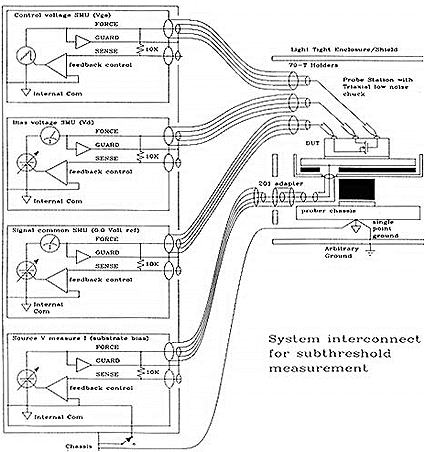
System grounds, shields, and connections
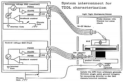
The ideal grounding, shielding and connection scheme for surface to surface and surface to substrate current measurements are shown in Figures 5 and 6.
Exploit filtering and averaging available in the instrument
Parametric measurements like subthreshold and TDDL lend themselves to filtering and averaging. Use these features to obtain a clean, nominal representation of these DC characteristics.
Guarding and settling time
The use of a guarded signal path will be a key contributor to successful low current measurements. The driven guard output on a typical SMU will provide a buffered output voltage that follows the source output. Since the voltage difference between the signal path and guard shield will be nearly zero, the leakage current through the isolation will be maintained at very low levels. Charging delay (settling time) of the signal line will be substantially reduced for the same reason. Refer to figure six and seven for the recommended guard configuration. Compensate for the remaining settling time by adding the appropriate measurement delay to the SMU.
Cable Isolation and noise
Femtoampere current measurements will require very high resistive isolation and guarding between the signal path and all conductors at the reference potential. Specify cabling designed for low leakage such as cable insulated with virgin PTFE (Teflon) insulation. Most cabling will generate some degree of intrinsic noise especially when the cable is flexed or vibrated, but most of this will subside after the motion stops. Cable designated as low noise is specifically manufactured to minimize triboelectric effects. When evaluating cables for leakage and intrinsic noise, allow the cable to relax into a limp position before making a leakage measurement. This requirement for a relaxed and motionless cable also applies when making real measurements. Note that the noise settling time could vary from seconds to tens of minutes depending on the cable type and characteristics.
Cleanliness
Avoid touching insulation between two conductors such as might be found around connectors, probes, shields, and guards. Oils or contamination on your fingers could cause an increase in leakage current.
Summary
The need exists for low current measurements in the range of 100 to 1 fA due to the continuing trend toward decreasing geometric scale. Instruments are now available that can resolve down to 1 fA or below, and engineers involved in process and design are ready to make use of this technology. The factors that affect the low current environment are well known and can be modeled as "virtual components." These models will help the visualization of noise sources and noise coupling mechanisms when trying to deduce and eliminate error sources in the test system. Because noise at the femtoampere level is difficult or impossible to see in real time, the best measure against this source of error is prevention.
- Best of Analog Dialog: Understanding Interference-Type Noise. A. Rich, Analog Devices, Inc.
- Best of Analog Dialog: Shielding and Guarding. A. Rich, Analog Devices, Inc.
- Noise Reduction Techniques in Electronic Systems. H. Ott, John Wiley and Sons.
- 1994 IEEE International Reliability Physics Proceedings: Stress-Induced Low-Level Leakage Mechanism in Ultrathin Silicon Dioxide Films Caused by Neutral Oxide Trap Generation. Kimura and Koyama.
- IEEE Transactions on Instrumentation and Measurement, VOL. 38, NO. 6, December 1989: A Compact Self-Shielding Prober for Accurate Measurement of On-Wafer Electron Devices. Yamamoto.
- Interfacing Micromanipulator Probe Stations to Your Measurement Equipment. Application Note, The Micromanipulator Co.
- Application Note 238: Semiconductor Measurements with the HP4140B Picoammeter/DC Voltage Source. Hewlett-Packard Corp.
- Application Note 315: Practical Applications of the HP 4145B Semiconductor Analyzer. Hewlett-Packard Corp.
- Application Note 356: High Speed DC Characterization of Semiconductor Devices from Sub pA to 1A. Hewlett-Packard Corp.
- Envisioning Your Test System? Watch for Error Sources. T. Mego, Keithley Instruments, Inc. R and D Magazine, September, 1992.
- Low Level Measurements Handbook, Keithley Instruments, Inc.
- Keithley 236/237 Source Measure Units Applications Overview. Keithley Instruments, Inc.
- Keithley Application Note Series: Low Level measurements. Keithley Instruments, Inc.
Acknowledgments
Special thanks to the following people for sharing their knowledge, experience and time:
Lee Stauffer; Keithley Instruments, Inc.
Jim Forst; The Micromanipulator Co., Inc.
Dan Harrison; The Micromanipulator Co., Inc.
For more information
Karen Schanhals
Advertising & Promotions Manager
The Micromanipulator Co., Inc.
1555 Forrest Way
Carson City, Nevada 89706 USA
Telephone: 775-882-2400
Fax 775-882-7694
info@micromanipulator.com